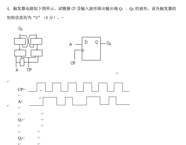
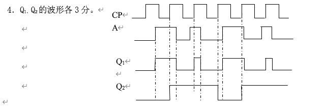
Latch 锁存器
S-R Latch S-R锁存器
S, R 分别代表 SET, RESET.
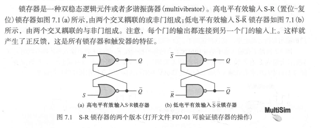
A latch (锁存器) is a temporary storage device that has two stable states (called bistable)—SET state and RESET state.
The S-R (Set-Reset) latch is the most basic type, and it can be constructed from NOR gates or NAND gates.
-
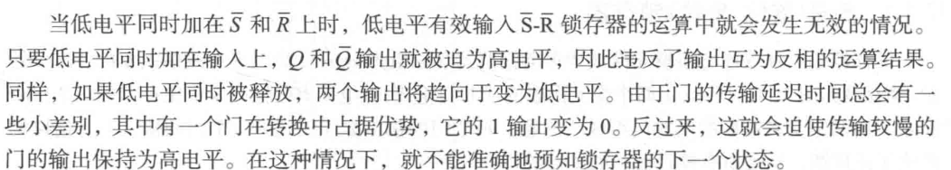
With NOR gates, it responds to active-HIGH inputs;
-
With NAND gates, it responds to active-LOW inputs.
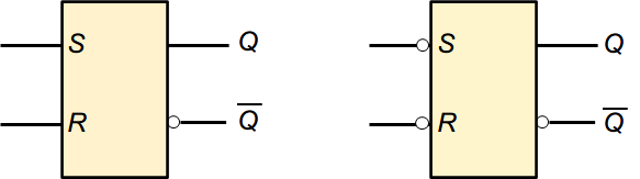
- is RESET.
- is SET.
Normal Operation
When a momentary LOW is applied to and remains HIGH, it turns from RESET to SET or remains SET.
When a momentary LOW is applied to and remains HIGH, it turns from SET to RESET or remains RESET.
Invalid Operation
Never apply active SET and RESET at the same time (invalid)!
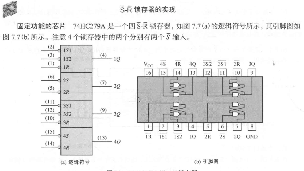
74LS279A
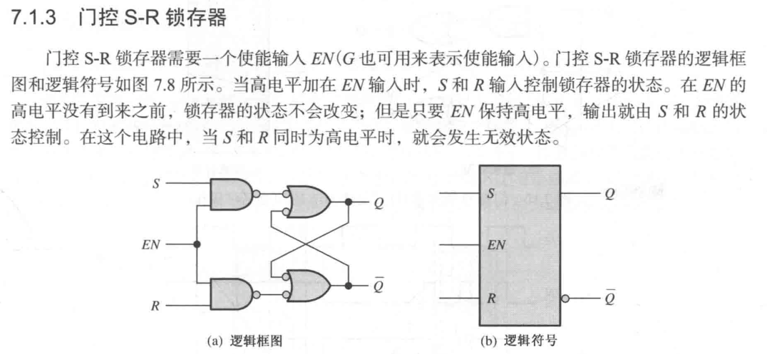
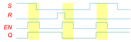
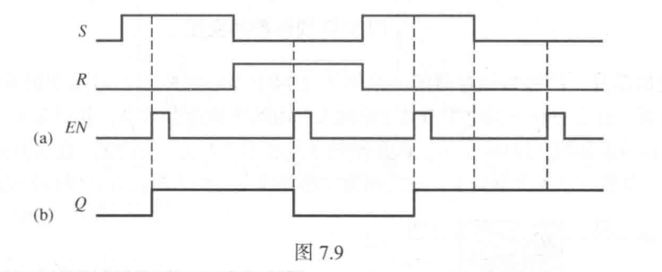
Gated S-R Latch 门控 S-R 锁存器
The gated (S-R) latch has an additional enable (EN) input that must be high in order for the latch to respond to the S and R inputs.
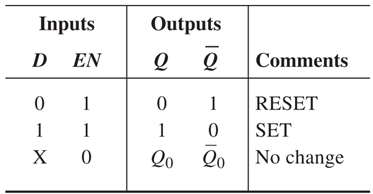
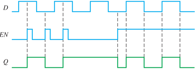
Gated D Latch (门控D锁存器)
The (gated) D latch is a variation of the gated latch with the S and R inputs combined to a single input D (D means “data”).
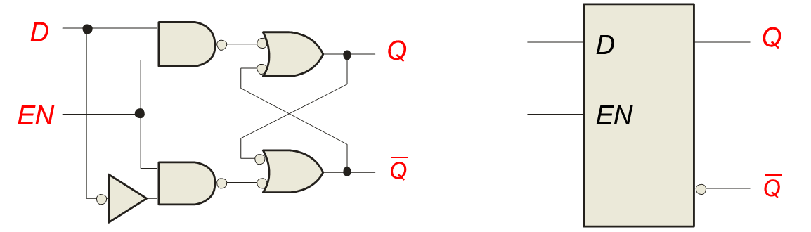
Rules for the D latch:
-
Q follows D when EN is active.
-
Q is latched when EN is inactive.
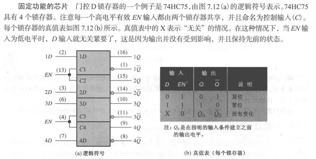
74HC75
74HC75 is an IC of four gated D latches. Each EN input is shared by two latches.
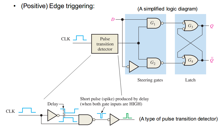
Edge-Triggered Flip-Flops (边沿触发器)
A flip-flop (触发器) is also a temporary storage device that has two stable states — SET state and RESET state.
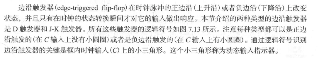
A flip-flop differs from a latch in the manner that it changes states.
-
A gated latch is level-sensitive in that its activeness is based on the EN level.
-
A flip-flop is edge-sensitive in that its activeness is based on the edge of a clock (CLK) input (the C input).
A flip-flop changes state
-
either at the rising edge of the clock ( called positive edge-triggered )
-
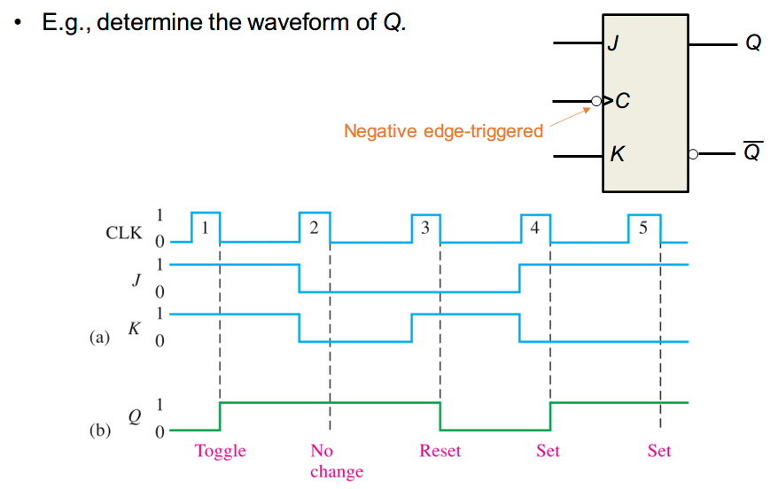
or at the falling edge of the clock ( called negative edge-triggered ).
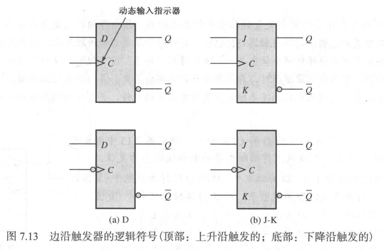
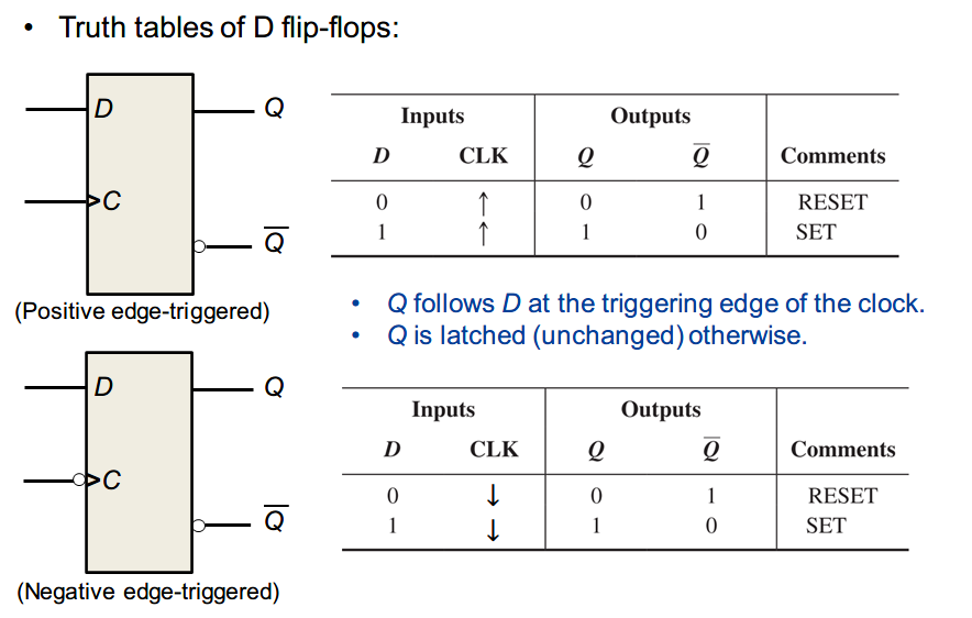
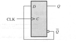
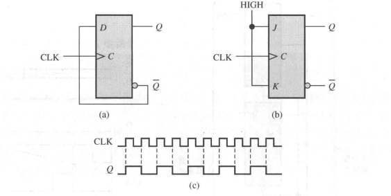
D Flip-Flops (D触发器)
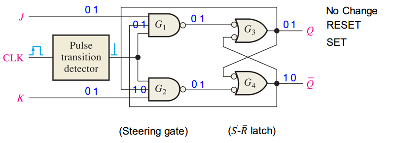
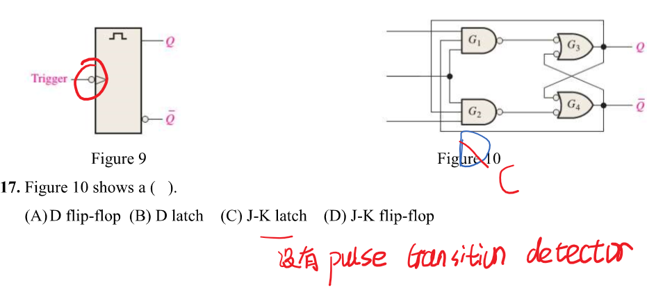
D 触发器的原理 EN Pulse Transition Detector.
实现 toggle 的功能。
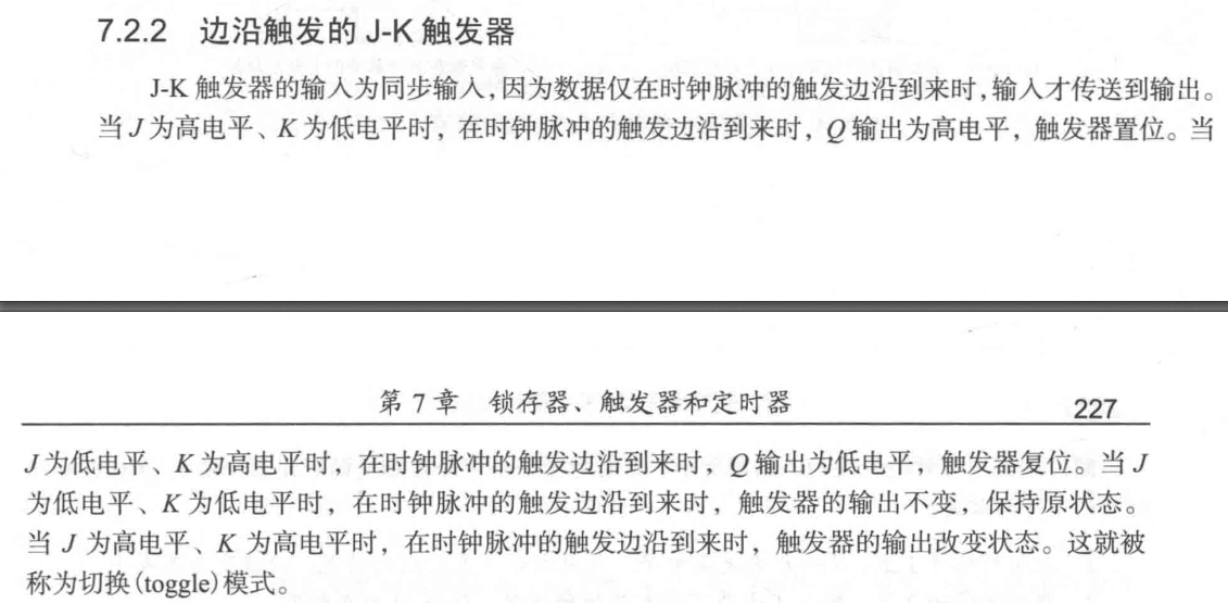
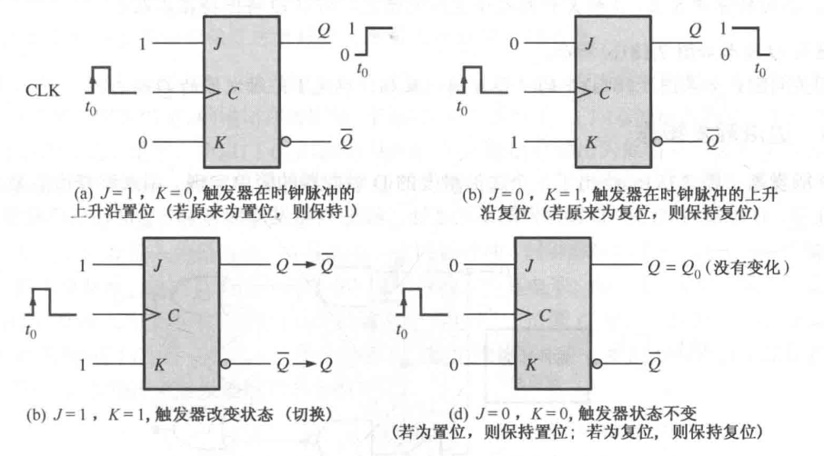
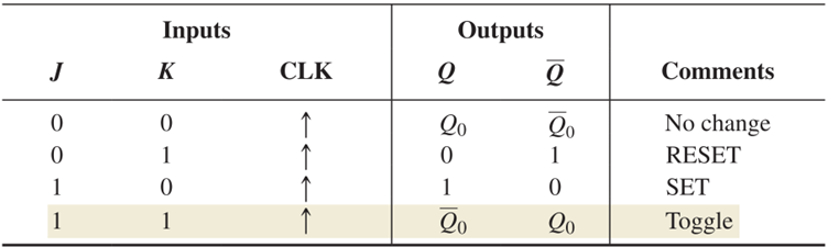
J-K Flip-Flops (J-K触发器)
The J-K flip-flop is more versatile than the D flip flop. (“J-K” is in honor of the inventor Jack Kilby.)
It has two data inputs J and K, which affect the output on the triggering edge of the clock.
When J = 1 and K = 1, the output changes states (the toggle (翻转) mode) on the triggering edge of the clock.
Hardwire a toggle mode in D flip-flop by connecting back to .


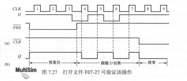
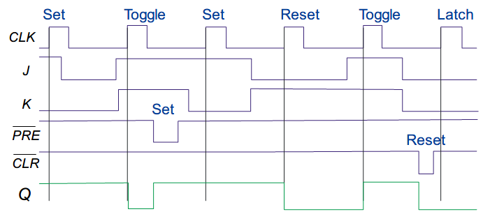
Asynchronous Preset and Clear (异步预置和清除)
The D or J-K inputs are synchronous inputs in that these inputs are transferred on the triggering edge of the clock.
Most flip-flops have other asynchronous inputs that affect the output independent of the clock. PRE: preset and CLR: reset. 相当于独立的一个 S-R 锁存器。

触发器运算特性 Flip-Flop Operating Characteristics
The performance, operating requirements, and limitations of flip-flops are specified by several operating characteristics or parameters.
-
Propagation delay time (传播延时)
-
Set-up time (设置时间)
-
Hold time (占用时间)
-
Maximum clock frequency (最大时钟频率)
-
Pulse width (脉冲宽度)
-
Power dissipation (功耗)
Propagation Delay Time (传播延时)
A propagation delay time is the interval of time required for the output change to occur after an input signal is applied.
Synchronous clock to output: It is measured from the 50% level of the clock to the 50% level of the output transition.
means LOW to HIGH, means HIGH to LOW.
Asynchronous preset/clear to output: It is also measured from the 50% level of the preset/clear input to the 50% level of the output transition.

Set-up Time and Hold Time (设置时间/占用时间)
The set-up time and hold time are times required before and after the clock transition that input data are reliably clocked into the flip-flop.


Flip-Flop Applications 触发器应用
Parallel Data Storage (并行数据存储)
Principal flip-flop applications are for temporary data storage, as frequency dividers, and in counters (covered in Chapter 9).
Typically, for data storage applications, a group of flip-flops are connected to parallel data lines and clocked together. Data is stored until the next clock pulse.

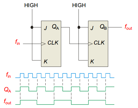
Frequency Division (分频)
For frequency division, simply use a flip-flop in the toggle mode or to chain a series of toggle flip flops to continue to divide by two.
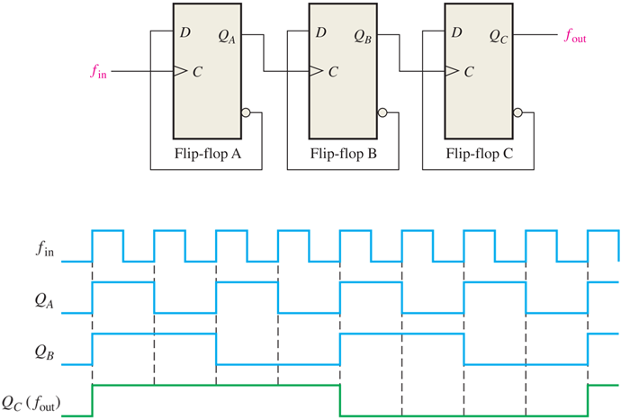
Counting (计数)
For counting, a series of toggle flip-flops are chained as for frequency division. The outputs of flip-flops are a binary sequence. (The J-Ks in the right example are negative edge-triggered.)

注意是负边缘触发,否则就是分频。
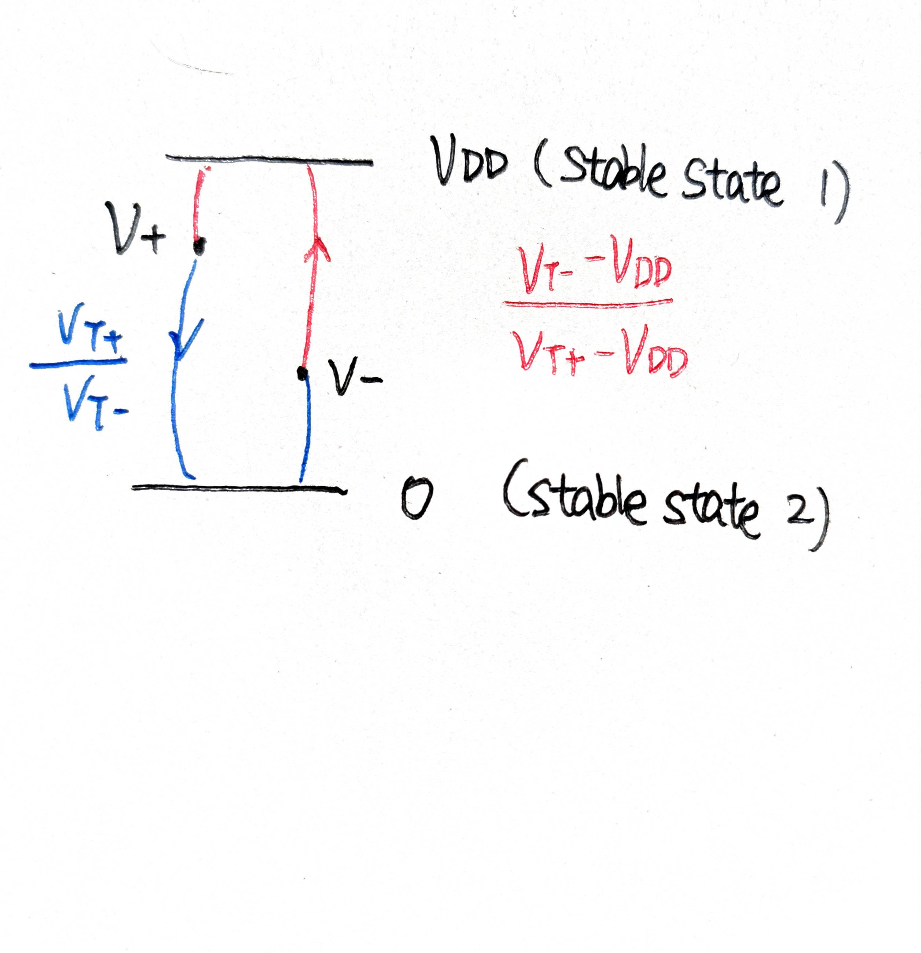
Schmitt Trigger (施密特触发器)
A Schmitt trigger is a special type of bistable devices that have two states—Two threshold voltages (阈值电压,参考电压).
- An upper threshold of the input driving LOW-to-HIGH output transitions.
- A lower threshold of the input driving HIGH-to-LOW output transitions.
A Schmitt trigger can generate rectangular pulses with sharp edges. Thus, it is useful for
- sharping slowly-varying signals, and
- increasing the noise immunity.
简单来说,施密特触发器可以将模拟信号转化为高低电平信号。
比较器也可以将模拟信号转化为高低电平信号。但是电压信号存在噪声,当输入电压接近参考电压时,就会产生许多波动,导致频繁地输出高低电平。
施密特触发器具有两个参考电压,当电压超过高参考电压时,输出高电平,此时的参考电压转化为低参考电压,当电压低于低参考电压时,输出电压才转换为低电平。


One-Shots 单稳态触发器
One-Shots (单稳态触发器)
之前的锁存器都是双稳态触发器。这里介绍单稳态触发器,只有低电平是稳态。
The one-shot (also called monostable multivibrator) has one stable state and one unstable state.
The one-shot is normally in its stable state and, once triggered, it changes to its unstable state and remains there for a predetermined length of time before returning to its stable state.
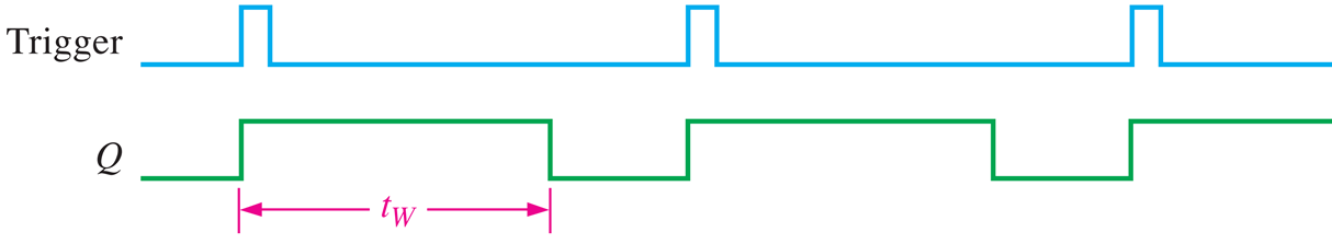
For a single trigger input, the duration of the unstable state is the pulse width (). (Note: The duration of the unstable state for a single trigger input is determined by circuit parameters, but not related with the triggering pulse.)
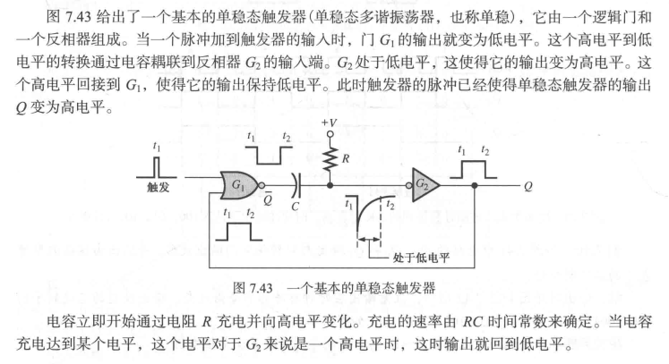
电容保持其电势差不变,一开始左右电势都是 HIGH,然后左边变成 LOW,右边也要变成 LOW。之后,慢慢充电,右边电势达到阈值的时候,即 时刻,输出 变为 LOW。左边电势 HIGH,右边电势保持电势差不变,变为 2*HIGH.

The duration of the LOW input of is determined by the time constant of the equivalent circuit.
The logic symbols with and without an external resistor (RX/CX) and capacitor CX.

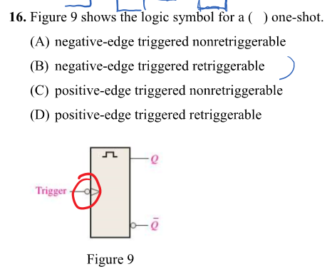
Nonretriggerable One-Shot 不可重复触发单稳态触发器
A nonretriggerable one-shot does not respond to any additional triggers from the time it is triggered until it returns to the stable state.
The duration that the one-shot remains in its unstable state is the pulse width of the output.

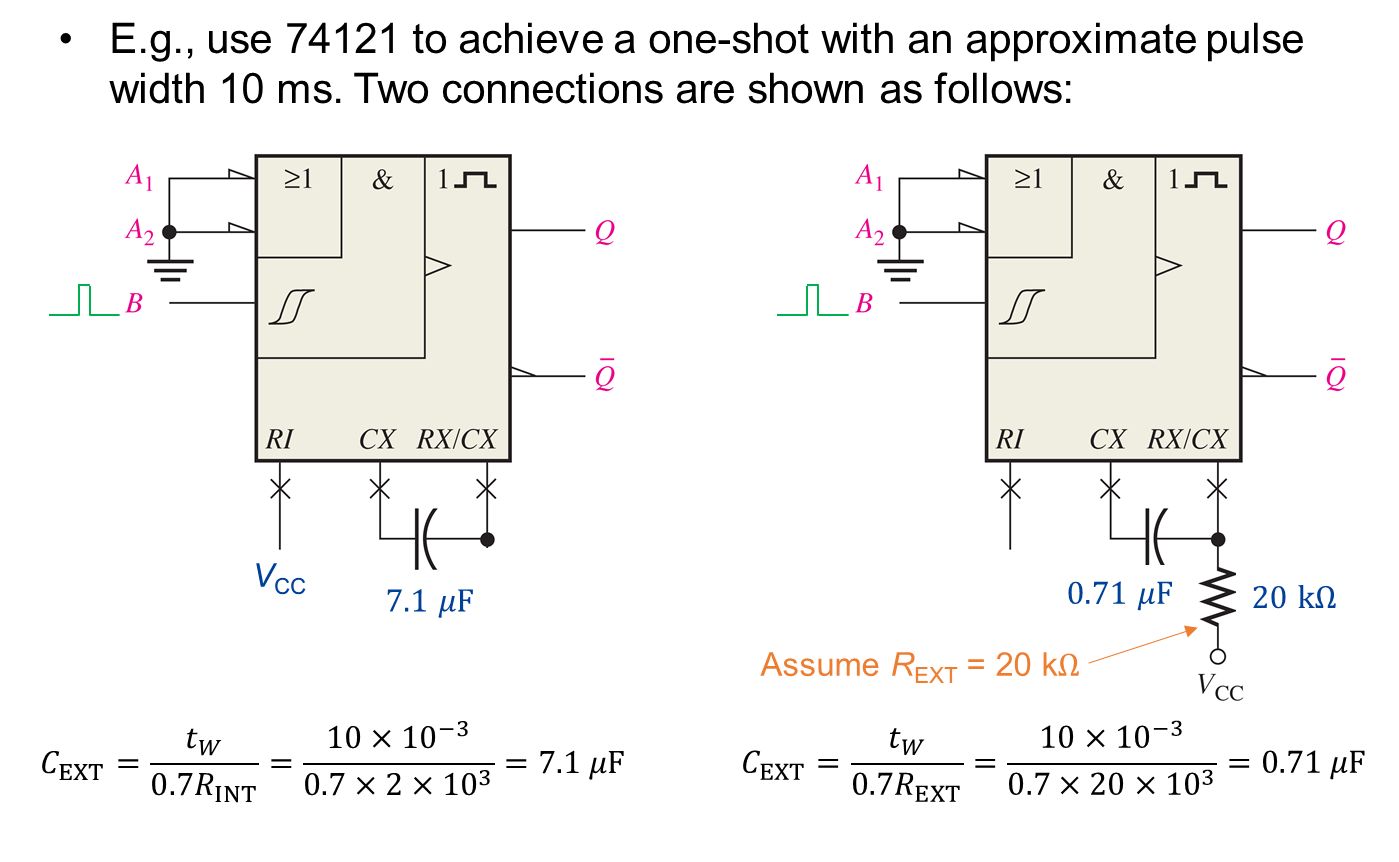
74121
不可重复触发的符号,含有一个 .


因为施密特触发器计算的是电压差。测量的是下减上。
Three connection ways for setting the pulse width of 74121:
-
Use the internal resistor without an external capacitor.
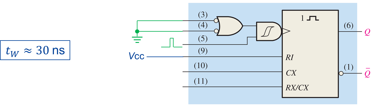
注意 RI 接高电平,原理见 One-Shots.
-
Use the internal resistor with an external capacitor

注意 接在 CX 和 RX/CX 之间,原理还是见 One-Shots. 利用 ,
Retriggerable One-Shot

74122


The Astable Multivibrator 非稳态多谐振荡器
An astable multivibrator (多谐振荡器, also known as pulse oscillator) has no stable states. It continuously switch between two unstable states without any external triggering.
The output of an astable multivibrator is typically used as a clock signal for the timing purpose.
This section does not fully cover Section 7.6 of the textbook.
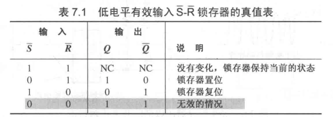
图 7.55 (a) 给出了一个简单形式的非稳态多谐振荡器,它使用一个有磁滞效应(施密特触发)的反相器和一个具有反馈连接的 RC 电路。当第一次加上电源时,电容上没有负荷,使得施密特触发的反相器的输入为低电平,输出位高电平。电容 通过电阻充电,直到输入电压达到高触发点(UTP)时,如图 7.55 (b) 所示。此时,反相器的输出为低电平,使得电容 通过电阻 放电。当反相器的输入电压降低到低触发点(LTP)时,输出变为高电平,电容 再次充电。只要没有断电,这个充电/放电过程一直重复下去,输出就是脉冲波形,如图中所给出的那样。


充电和放电通过不同的电阻。
Charge and Discharge.
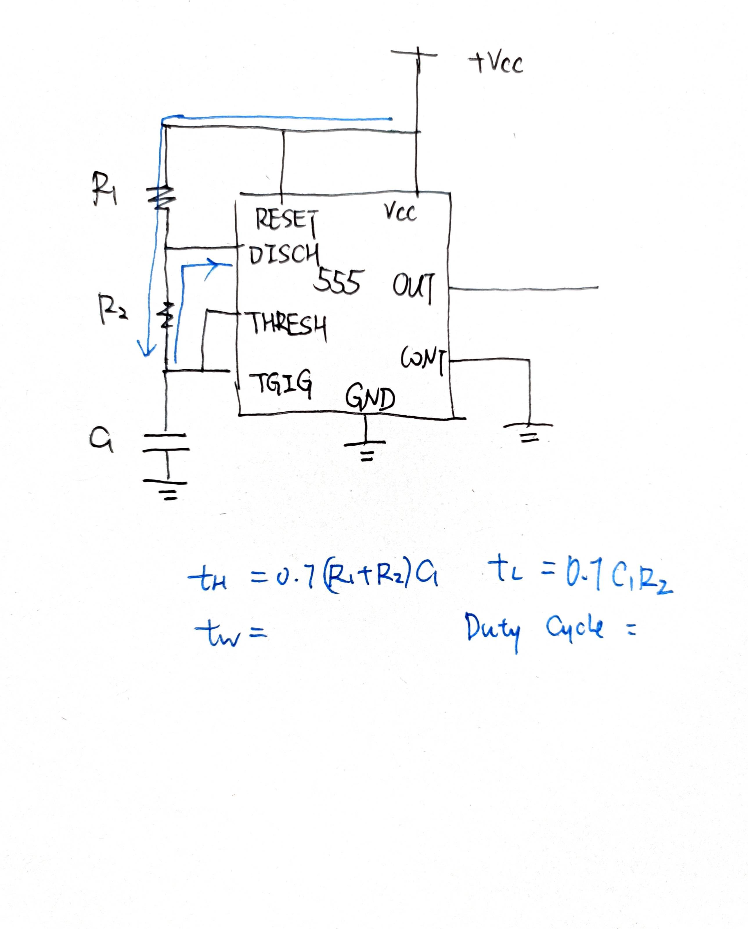
When , Fixed duty cycle: when .
The duty cycle can be adjusted by selecting proper and .
The 555 Timer(555定时器)
The 555 timer is an analog-digital-mixed device, and it is versatile because it can be configured in three different modes as a Schmitt trigger, a one-shot, or an oscillator.
Although it was firstly marketed in 1972, over a billion chips were produced annually by some estimates in 2017, and it was said to be “probably the most popular integrated circuit ever made” (Wikipedia).
Comparator

Discharge Transistor(放电晶体管/三极管)

The 555 Timer

Voltage

The latch and the discharge transistor

555 Timer as a Schmitt Trigger
高参考电压。
低参考电压。
加上电容是为了稳定参考电压。

555 Timer as a One-Shot
Non retriggerable One-Shot.


这里降到原来电压的三分之一才能触发,所以前面系数是 。
555 Timer as an Astable Multivibrator


-
Charge 通过两个电阻
-
Discharge 通过一个电阻
如果加上二极管,使得充电只经过 呢??